In the professional LED display industry, buyers often obsess over pixel pitch, refresh rates, and the peak brightness of LED lamps. However, the most critical element for structural stability, chromatic consistency, and long-term lifespan is hidden deep within the module: the PCB (Printed Circuit Board). Far more than just a mounting surface, the PCB acts as the "Central Nervous System" and "Thermal Foundation" of the screen. In this technical encyclopedia, we explore why this humble board dictates whether your display remains an asset for a decade or becomes a liability in six months.
1. Engineering Anatomy: PCB vs. PCBA Definitions
Understanding the distinction between PCB and PCBA is fundamental to LED procurement. A PCB (Printed Circuit Board) is a passive carrier—a complex "sandwich" of copper, resin, and fiberglass. Its primary function is to provide physical support and a pre-defined electrical highway for electrons. According to the IPC-6012 standard, the raw PCB quality determines the success of all subsequent assembly phases.
A PCBA (Printed Circuit Board Assembly) is the fully populated, functional unit. This stage involves the SMT (Surface Mount Technology) process, where robotic arms place LED lamps and driver ICs at high speed. The reliability of the PCBA is directly tied to the PCB’s Surface Finish. Whether using ENIG (Electroless Nickel Immersion Gold) or OSP (Organic Solderability Preservative), the finish dictates the molecular bond strength of the solder joints. If this bond is weak, thermal expansion will cause "Micro-cracks," leading to dead pixels.
2. Material Science: Layers, Substrates, and Dielectrics
An LED PCB is a thermodynamic system. Its layers must work in harmony to prevent failure during intense heat cycles. Below are the core components:
- Base Material (Substrate): Most LED screens use FR-4 (Flame Retardant level 4). However, for high-end applications like Fine Pitch or COB, we may use Polyimide or Ceramic to meet high-frequency requirements.
- Copper Layer: The conductive highway. Measured in ounces (oz), standard boards use 1oz (35μm), while professional boards utilize 2oz (70μm) for better current capacity and heat transfer.
- Pad & Vias: Pads allow for component soldering, while Vias (Through-hole, Blind, or Buried) connect different circuit layers.
- Solder Mask: The protective polymer skin. While aesthetically green in most cases, it provides a 500V+ dielectric barrier and prevents oxidation of the copper traces.
3. Thermal Dynamics: Fourier’s Law and Copper Weight Selection
LED lamps are heat-sensitive semiconductors. As the junction temperature rises, light output decreases and the wavelength shifts, causing color distortion. The PCB is the primary thermal conductor tasked with moving this heat away from the lamps. This process is governed by Fourier’s Law of Heat Conduction:
Where: Q = Heat Flux | k = Thermal Conductivity | A = Cross-sectional Area | dT/dx = Temp Gradient
By increasing the Copper Weight from 1oz to 2oz, we effectively double the cross-sectional area (A) for heat conduction. This allows the PCB to carry twice the heat flux, reducing the junction temperature of the LED lamp by up to 15°C. For every 10°C reduction, the aging process is effectively halved, doubling the reliable life of the screen.
Technical Comparison: Standard vs. Professional Grade PCB Performance
| Feature | Standard Grade (Low Cost) | Professional Grade (High-End) | Technical Impact |
|---|---|---|---|
| Base Material | Low-Tg FR-4 (130°C) | High-Tg FR-4 (170°C+) | Prevents board warping and via-cracking in high heat. |
| Copper Thickness | 0.5oz - 1oz | 2oz (70μm) Minimum | Doubles thermal conductivity and stabilizes signal voltage. |
| Surface Finish | HASL (Tin Spray) | ENIG (Immersion Gold) | 10x higher oxidation resistance for long-term solder joint health. |
| Layout Density | Standard Pitch | High-Density (HDI) | Ensures signal integrity for 4K/8K Fine-Pitch displays. |
4. Fabrication Mastery: The Critical Manufacturing Stages
A reliable PCB is the result of chemical and mechanical precision. The process begins with Substrate Cutting and CNC Drilling. These micro-vias connect signal layers to power planes. Following drilling, Electroless Copper Deposition creates a conductive path within the holes.
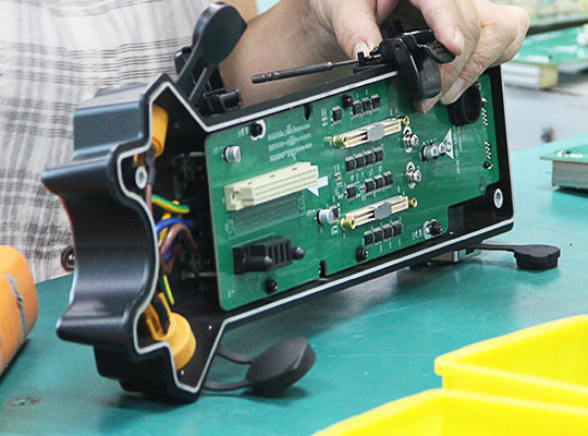
[Image showing the PCB manufacturing process including etching, drilling, and AOI testing]Crucial to signal integrity is the Etching phase. If the chemical bath is not perfectly controlled, "Under-cutting" occurs, where the traces become thinner than designed, increasing resistance. The final **Surface Treatment**—often Immersion Gold—provides a perfectly flat surface for SMT placement, ensuring that every 0.5mm LED lamp bead is perfectly aligned and electrically sound.
5. FMEA: Failure Mode Analysis of Substandard PCBs
Choosing a cheap PCB leads to irreversible hardware degradation. Here is what happens at a molecular level when engineering standards are ignored:
Critical Failure Modes (FMEA Analysis):
- CAF (Conductive Anodic Filament): In high-humidity environments, copper ions migrate along fiberglass fibers, creating internal shorts. This causes permanent "dead lines" on the display.
- The Popcorn Effect: Low-Tg resins absorb moisture. During operation, heat turns this moisture to steam, physically delaminating the board layers.
- Impedance Mismatch: Cheap PCBs fail to control trace width accurately. This causes signal reflections, manifesting as "Ghosting" or "Flickering," regardless of the control system quality.
6. Total Cost of Ownership (TCO): The Price of Quality
The PCB typically accounts for **10% to 20%** of the total LED module cost. By choosing a board that is 20% cheaper, a manufacturer might save $50 per square meter. However, the resulting failures lead to bucket-truck repairs and brand damage that exceed those initial savings by 10-fold.
At VMX Visual, we view the PCB as an insurance policy. A high-quality board ensures that the expensive LED chips operate in a stable, cool environment. This is the only path to achieving a true 10-year ROI for your visual asset.
7. Technical FAQ: Expert Procurement Checklist
Q: Why is the green solder mask so common?
Green is the industry standard because it offers the highest contrast against white silk screen and copper traces, making Automated Optical Inspection (AOI) more accurate. However, for high-end boutique screens, Black or White is often used for aesthetics.
Q: How can I verify if a supplier is using 2oz copper?
Request a cross-section report (Micro-section) of the PCB. A professional supplier should provide a measurement showing the copper thickness is ≥70μm for high-performance layers.
Engineering Reliability into Every Pixel
Don't let a "hidden" component compromise your brand's vision. We invite you to explore our full range of innovative visual solutions to find the perfect fit for your next project.
Explore Our High-Performance Products


Share:
ISE 2026 Wrap-Up: Innovation and Global Partnerships at VMX Visual
Lunar New Year Holiday Schedule 🏮