Pro-AV Technical Resource Quick Navigation
01 Pixel Pitch Generations | 02 SMT & Protective Packaging (SMD, GOB, COB) | 03 Micro-LED Milestones (MIP, CSP, COG) | 04 Silicon Topography & Thermal Dynamics
The professional LED display sector is undergoing rapid structural evolution. For global Pro-AV systems integrators, architectural consultants, and procurement directors, navigating the dense matrix of technical terminology—ranging from packaging topologies like COB and MIP to electrical drive architectures like common-cathode—is paramount. This master reference guide deconstructs the foundational hardware mechanics, silicon-level packaging, and power optimization frameworks driving the modern digital signage ecosystem.
To establish baseline standardization within engineering blueprints, display dimensions are classified strictly by their physical pixel spacing (pitch) and individual semiconductor die geometries:
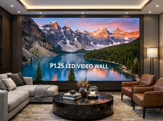
- Fine Pitch LED : Refers to standard high-density indoor displays featuring a physical pixel center-to-center distance (dot pitch) generally ranging between P1.0mm and P2.0mm. This baseline setup serves conventional control rooms, broadcast studios, and corporate boardrooms.
- Mini LED: Defined by semiconductor die nodes measuring between 50 and 200 micrometers (μm). The structural array maintains a pixel center-to-center pitch within the narrow operating envelope of 0.3mm to 1.5mm, frequently deployed for high-density direct-view displays and premium liquid crystal backlighting modules.
- Micro LED: Represents the current frontier of micro-optoelectronics, where individual LED chip configurations scale down below 50 micrometers (μm), and pixel center-to-center spacing drops **below 0.3mm**. This architecture delivers near-infinite contrast and exceptional pixel density.
- MLED: An industry-standard umbrella term combining **Mini LED** and **Micro LED** technological classifications into a unified, high-density emissive matrix category.
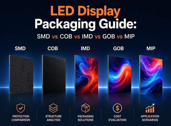
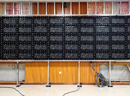
1. SMD (Surface Mounted Devices)
SMD technology encapsulates components like the cup, metallic subframe, semiconductor dies, internal wiring, and epoxy resin housing into discrete lamp beads. These individual packages are mounted onto printed circuit boards (PCBs) via high-speed Surface Mount Technology (SMT) and secured through high-temperature reflow soldering ovens.
Standard fine-pitch SMD modules leave the solder joints exposed or protected only by a plastic louver mask. While SMD remains the dominant commercial protocol due to mature manufacturing pipelines, low manufacturing costs, excellent thermal dissipation, and easy individual pixel rework, it has inherent physical vulnerabilities. Exposed components are prone to accidental impact damage, silver migration shorts, and pixel failures like "caterpillar" short circuits, which limit its suitability for high-end, touch-interactive public spaces.![]()
2. IMD (Integrated Matrix Devices)
IMD represents a transitional, multi-in-one matrix integration bridge separating traditional SMD packages from true solid-state COB arrays. Most common configurations utilize a 2×2 element architecture (4-in-1 bead layout) that pre-encapsulates 12 independent RGB semiconductor dies within a unified subframe.
This approach allows pixel pitches to scale down to **P0.7mm** while structural shear strength is significantly improved compared to standalone SMD beads. However, because multiple pixel nodes are bound together, individual binning for precise color matching and brightness uniformity becomes complex, requiring extensive pixel-level calibration to eliminate batch chromatic deviation.![]()
3. GOB (Glue On Board) & VOB (Vacuum Optional Layer) Protective Innovations
GOB applies a specialized protective polyurethane or epoxy potting layer across the front face of assembled SMD modules. This transparent coating encapsulates the exposed lamp beads and gaps, forming an isotropic shield that protects fragile surface arrays from liquid ingress and mechanical impact.
This process creates highly durable modules that resist moisture, dust, static, impact, and oxidation, making them well-suited for demanding rental applications. However, GOB layers can introduce challenges such as internal thermal stress buildup, localized yellowing, and difficult pixel-level repairs once the protective material cures.
To address these challenges, **VOB (Vacuum Optional Board)** premium coating technology uses specialized imported nano-resins applied via precise automated vacuum machinery. This approach delivers a significantly thinner, highly uniform layer that improves heat dissipation while enhancing contrast, reducing black-screen color shift, and maintaining high reliability.![]()
4. COB (Chip on Board) Semiconductor Architecture
COB bypasses individual packaging subframes entirely by **bonding bare emissive semiconductor dies directly onto the PCB substrate**, establishing electrical contacts via ultra-fine wire bonding or flip-chip connections before sealing the entire module surface under a protective optical resin layer.
This solid-state panel design provides exceptional mechanical durability, high static discharge protection, and superior contrast performance. Eliminating exposed wire links significantly drops failure rates compared to standard SMD layouts. Its excellent heat transfer path makes COB an ideal technology pathway for the modern Mini LED generation.![]()
As the industry targets sub-0.5mm pixel configurations, physical limitations in handling ultra-small components require advanced manufacturing approaches:
1. COG (Chip on Glass)
COG technology mounts bare emissive semiconductor dies directly onto a **glass substrate (TFT backplane)** instead of a traditional flexible or composite resin PCB. This structural shift allows layout tolerances to drop **below P0.1mm** due to the superior thermal stability and flatness of glass, positioning COG as a prime structural pathway for ultimate Micro LED commercialization.
2. MIP (Module in Package)
MIP slices high-density sub-wafers into discrete micro-packages before execution of SMT layout steps. By grouping RGB micro-dies into single-pixel or multi-pixel integrated packages, MIP addresses mass transfer yield bottlenecks, allowing standard inspection machinery to test and bin pixels prior to final module layout.
3. CSP (Chip Scale Package)
CSP represents a highly compact evolution of surface-mount components, engineered to minimize package size down to roughly 1.2 times the native silicon footprint. Designed primarily for flip-chip architectures, CSP eliminates internal wire bonds and subframe housings, enclosing the die within a minimized protective resin shell that balances packaging yield with low repair costs.
1. Wire-Bonded (Face-Up) vs. Flip-Chip (Face-Down) Silicon Structures
The positioning of positive and negative contact electrodes on the silicon die determines its long-term reliability and optical efficiency:
Traditional **wire-bonded (face-up) chips** feature the contact electrodes and primary emissive face on the same upper surface. Electrical connections are established using ultra-fine gold or copper wire loops bonded to the underlying PCB. A standard three-color RGB pixel can require up to five independent wire loops. Under thermal cycling and physical stress, these delicate wire bonds can break or lift, leading to open circuits and dead pixels.
Conversely, **flip-chip (face-down) architecture** inverts this topography. The contact electrodes face downward, bonding directly to the underlying PCB contact pads via conductive solder bumps, while the primary light-emitting surface faces upward without obstruction. This layout eliminates delicate wire loops, significantly enhancing mechanical stability, optimizing the thermal path to the substrate, and maximizing light extraction efficiency.
2. Asynchronous vs. Synchronous Network Control Topologies
- Synchronous Control Networks: Map display content pixel-for-pixel in real-time with an external video source, such as a dedicated media server or PC workstation. If the primary connection is interrupted, the display stops rendering, making this setup standard for high-density indoor control rooms and broadcast studios.
- Asynchronous Control Networks: Feature onboard processing and flash memory storage. Media assets are uploaded remotely via 5G, Wi-Fi, or physical USB storage, allowing the display network to operate independently of a continuous media server link—a critical requirement for permanent outdoor billboards.
3. Common-Anode vs. Common-Cathode Power Distributions
Power management architectures directly impact thermal generation and overall system efficiency:
Standard **common-anode distribution** routes a uniform 5V power line to the positive terminals (anodes) of the Red, Green, and Blue LED dies. Because individual colors require different forward operating voltages—Red typically operates around 2.8V, while Green and Blue require roughly 3.8V—the excess voltage supplied to the Red die must be dissipated through dropping resistors. This conversion turns the unneeded voltage into waste heat, lowering system efficiency.
Advanced **common-cathode architecture** solves this inefficiency by grouping the negative terminals (cathodes) together and splitting the positive power lines into independent, voltage-matched rails. By supplying 2.8V directly to the Red die and 3.8V to the Green and Blue dies, dropping resistors are eliminated.
This direct matching **reduces power consumption by 25% to 40%** and significantly lowers operating temperatures. Lowering heat generation minimizes thermal wavelength drift, ensures consistent color accuracy, and extends the operating lifespan of high-density panels, especially when paired with solid-state COB arrays.
| Topology Class | Primary Physical Advantages | Inherent Technical Constraints | Optimal Pro-AV Deployment Target |
|---|---|---|---|
| SMD | Highly mature supply chain; low cost; simple individual pixel rework. | Low impact resistance; susceptible to silver migration and environmental degradation. | Conventional cost-sensitive commercial signage (P1.5mm - P4.0mm). |
| COB | Exceptional impact protection; superior contrast; low pixel failure rates. | Complex batch color calibration; challenging onsite module-level repairs. | Premium interactive smart classrooms, executive boardrooms, control centers. |
| MIP | High yield verification pre-assembly; uniform color consistency. | Requires high-precision SMT alignment; complex packaging steps. | Ultra-fine direct-view command consoles (Sub-P0.9mm direct-view). |
Technical Procurement Summary
Designing a modern digital signage network requires carefully matching packaging technology to the installation environment. For public spaces and educational touch-interactive installations, prioritizing **COB or protective VOB/GOB layers** offers necessary mechanical durability and impact mitigation. In control rooms demanding fine pixel density, **MIP and flip-chip architectures** provide high visual uniformity and electrical stability. Finally, for high-density applications, specifying **common-cathode power routing** is essential to control system temperatures, prevent color drift, and optimize long-term return on investment (ROI).
Q: Why does common-cathode drive routing resolve chromatic wavelength drift during prolonged direct-view usage?
In common-anode systems, excess voltage routed to the Red silicon die is converted into waste heat via dropping resistors, leading to uneven thermal patterns across the module. This heat shifts the operational junctions of the LED dies, causing the Red light wavelength to drift and distorting color accuracy. By supplying independent, voltage-matched rails to each die, common-cathode architecture keeps panel operating temperatures up to 15°C lower, eliminating thermal color drift and ensuring precise, stable color reproduction.
Q: How does MIP technology resolve mass transfer limits in sub-P0.5mm Micro LED production compared to true COB?
True COB requires transferring millions of raw, unshelled micro-dies directly onto a large PCB substrate with micron-level placement precision. A single positioning error or bad die can ruin an entire assembled module. MIP solves this by separating high-density sub-wafers into small, pre-packaged pixel cells. These cells can be fully tested, binned, and verified using standard automated optical equipment before final surface mounting, significantly reducing manufacturing defects and scaling challenges for sub-P0.5mm screens.
Q: What causes the "caterpillar" short-circuit phenomenon in fine-pitch SMD displays, and how do solid-state panels prevent it?
The "caterpillar" phenomenon occurs when an individual LED pixel suffers an internal short or a solder point bridges under high moisture and static conditions. This short creates an unintended current path along the shared drive column or scan line, causing a row of adjacent pixels to lock into a single color state that resembles a caterpillar track. Solid-state panels like COB eliminate exposed surface pins, solder joints, and open subframes within an integrated epoxy matrix, blocking moisture paths and reducing column short circuits.
Regulatory Standards & Engineering Compliance
- IEC 60529 — Ingress Protection (IP65 front / IP54 rear structural encapsulation verification).
- IEEE 1789-2015 — Recommended practices for modulating current in high-brightness LEDs to mitigate health risks from flicker patterns.


Partager:
How to Choose Campus LED Displays: 4 Sourcing Tips for Smart Schools